Phone(+65) 6284 3818 | sales@premier-sols.com | Enquriy |
FSM 127
Description
Optical Measurements Techniques - Imaging Low Coherence Interferometry
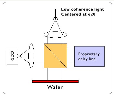
High-Resolution Nano - Topography for Flatness and Local Stress
Features
- Non-contact
- Imaging
- Nano-Topography and Local Stress measurement
- Die and Wafer Topography measurement capability
- Large working distance (10 mm or more)
- High lateral and height resolution
|
Localized Stress Measurement |
Inputs to stress measurement w/ FSM 127 system
|
Output
|
Configurations The following Configurations are available:
|
Premier Solutions Pte Ltd / FSM 127 - Optical Measurement


