Phone(+65) 6284 3818 | sales@premier-sols.com | Enquriy |
FSM 413
Description
Optical Measurement Techniques - Wafer Thickness
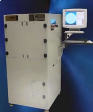
The FSM 413 EchoprobeTM sensor uses patent pending infrared (IR) interferometric technique, which provides a direct and accurate map of thick to ultra-thin wafers measurement of substrate thickness, and thickness variation (TTV). Several materials transparent in IR beam, such as Si, GaAs, InP, SiC, Glass, Quartz and many polymers are readily measured with standard spatial resolution of 60 microns spot, (smaller spot sizes are available). Using a Single probe system, substrate thickness of conventional wafers with patterns, tapes, bumps or bonded wafers mounted on carriers can be determined with high precision and accuracy. When configured as a Dual probe system, the FSM413 also provides measurements of total thickness of the wafer, including substrate thickness and the patterned height thickness. Options are available to measure wafer warp, trench depth and via holes, including high aspect ratio trenches and vias in MEMs type applications. Various specialized MEMs applications including membrane metrology are also available.
Premier Solutions Pte Ltd / FSM 413 (Optical Measurement)


